In the heart of the semiconductor industry, California stands out as a global leader in innovation and technological advancements. One critical aspect of this thriving industry is the probe card manufacturing process, a cornerstone for semiconductor testing. Probe cards play a pivotal role in ensuring the functionality and reliability of semiconductor devices, making their production a vital aspect of the tech ecosystem.
With California’s renowned expertise in microelectronics and cutting-edge manufacturing techniques, the state has become a hub for the development and production of probe cards. This article explores the intricate process behind probe card manufacturing, shedding light on its importance, methodologies, and the role California plays in advancing this technology.
Understanding the Role of Probe Cards in Semiconductor Testing
Probe cards serve as an interface between the testing equipment and the semiconductor wafer. They enable electrical signals to be transmitted, allowing manufacturers to assess the functionality of integrated circuits (ICs) before they are packaged. This step is crucial in detecting defects, ensuring product quality, and reducing waste in the manufacturing process.
The increasing complexity of semiconductor devices, coupled with the demand for smaller and more powerful components, has driven advancements in probe card technology. Modern probe cards are designed to accommodate higher pin counts, finer pitches, and advanced testing requirements, reflecting the evolving needs of the semiconductor industry.
Key Steps in the Probe Card Manufacturing Process
1. Design and Development
The manufacturing process begins with an in-depth design phase. Engineers collaborate with clients to understand the specific requirements of the semiconductor devices to be tested. These parameters include wafer size, pin configuration, and testing conditions.
Using sophisticated computer-aided design (CAD) software, engineers create detailed blueprints of the probe card. This stage involves meticulous planning to ensure the probe card meets the performance and durability standards required for high-precision testing.
2. Material Selection
Selecting the right materials is critical for the performance and longevity of probe cards. The base substrate, typically made of ceramic, epoxy, or fiberglass, must exhibit high electrical insulation and mechanical stability. Probe needles or contacts, usually crafted from tungsten, beryllium copper, or other conductive materials, are chosen for their electrical conductivity and resistance to wear.
In California, manufacturers often leverage locally sourced, high-quality materials, contributing to the state’s reputation for producing reliable and durable probe cards.
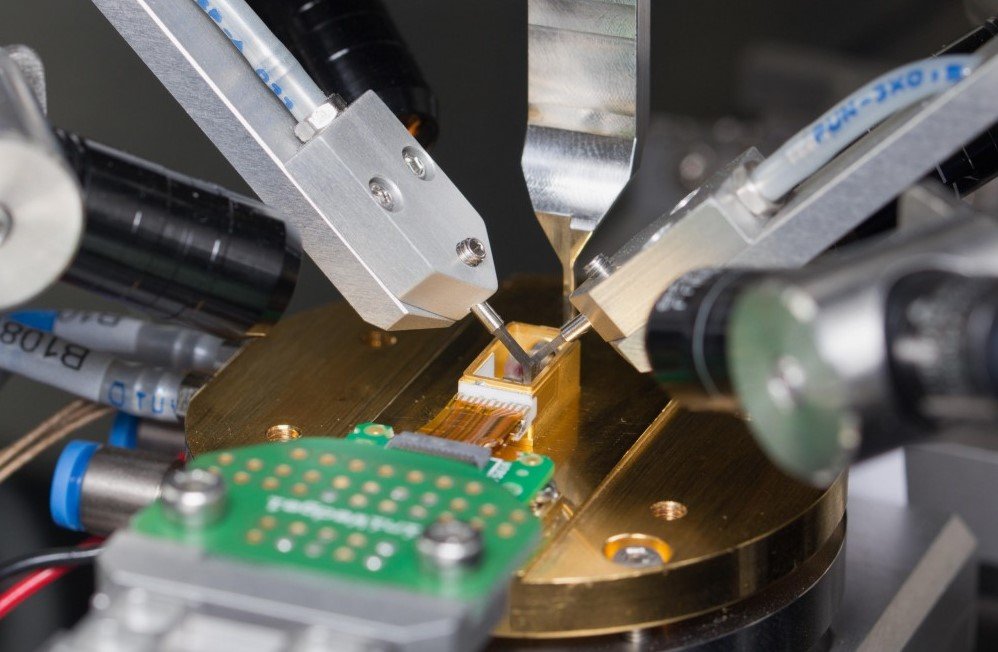
3. Microfabrication of Probe Needles
The probe needles, which make direct contact with the semiconductor wafer, undergo a precise microfabrication process. Techniques such as photolithography and chemical etching are employed to achieve the required dimensions and alignments. The goal is to create needles that can withstand repeated testing cycles without compromising accuracy or performance.
California’s advanced microfabrication facilities and skilled workforce ensure that this step is executed with exceptional precision, aligning with the stringent demands of the semiconductor industry.
4. Assembly of the Probe Card
Once the components are prepared, the probe card is assembled. This involves mounting the probe needles onto the substrate and aligning them according to the design specifications. Automated systems and skilled technicians work in tandem to ensure the accuracy of this alignment.
The assembly process also includes securing the components to withstand the mechanical stress of repeated testing. Manufacturers in California utilize state-of-the-art equipment and quality control measures to maintain the integrity of the probe cards.
5. Testing and Calibration
Before probe cards are shipped to clients, they undergo rigorous testing and calibration. This step ensures that the probe cards can perform accurately under various testing conditions. Parameters such as contact resistance, alignment accuracy, and durability are assessed.
California’s manufacturers leverage advanced testing facilities equipped with cutting-edge technologies to verify the performance of their probe cards. This commitment to quality underscores the state’s leadership in the semiconductor testing industry.
6. Customization and Delivery
Probe card manufacturers often provide customization options to meet the unique needs of their clients. Whether it’s adjusting the needle configuration or enhancing the card’s thermal resistance, customization ensures that the probe cards deliver optimal performance for specific applications.
Once the final product passes all quality checks, it is packaged and delivered. California-based manufacturers pride themselves on their ability to meet tight deadlines while maintaining the highest quality standards.
The Importance of California’s Expertise in Probe Card Manufacturing
California’s dominance in the semiconductor industry is supported by its robust infrastructure, skilled workforce, and commitment to innovation. The state is home to numerous research institutions, fabrication facilities, and testing labs that drive advancements in probe card technology.
Manufacturers in California benefit from proximity to leading semiconductor companies, fostering collaboration and enabling rapid development of new technologies. This ecosystem not only supports the production of high-quality probe cards but also positions California as a global leader in semiconductor testing solutions.
Future Trends in Probe Card Manufacturing
As the semiconductor industry continues to evolve, probe card manufacturers face new challenges and opportunities. The shift toward advanced packaging, including 3D stacking and heterogeneous integration, requires probe cards with even greater precision and complexity.
California’s manufacturers are at the forefront of addressing these demands, investing in research and development to create next-generation probe cards. Innovations such as MEMS-based probe cards and optical probing solutions are poised to revolutionize the industry, further solidifying California’s role as a leader in semiconductor testing.
Conclusion:
The probe card manufacturing process is a sophisticated and essential aspect of the semiconductor industry. From design and material selection to assembly and testing, each step is executed with precision to ensure the reliability of semiconductor devices. California’s expertise and infrastructure play a pivotal role in advancing probe card technology, meeting the growing demands of this dynamic industry.